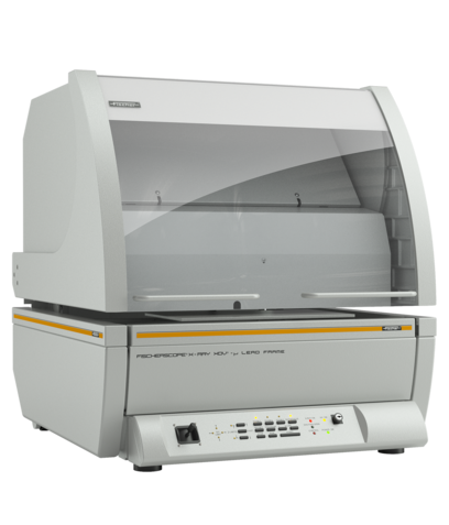
FISCHER FISCHERSCOPE X-RAY XDV-μ LEAD FRAME Coating Thickness Meter (Ø 50 µm halofree*)
Helium flush allows for measurement of even very light elements starting at sodium
Polycapillary optics
High-power tubes with chrome anode
4-fold automatically exchangeable filter
High-resolution CCD color camera, crosshairs with calibrated scale, adjustable LED illumination and laser pointer (class 1) for exact sample placement
Silicon drift detector
Fast, programmable XY-stage with pop-out function and electrically driven Z-axis for automated measurements
Applications
Au/Pd/Ni/CuFe and Sn/Ni coatings in the micro- and nanometer range
Assembled and unassembled circuit boards
Testing of base metallization layers (under-bump metallization, UBM) in the nanometer range
Measurement of light elements, e.g. determination of the phosphorus content (in ENEIG/ENEPIG) under Au and Pd
Lead-free solder caps on copper pillars
Testing the elemental composition of C4 and smaller solder bumps, as well as small contact surfaces in the semiconductor industry
Brochure
Get exclusive volume discounts, bulk pricing updates, and new product alerts delivered directly to your inbox.
By subscribing, you agree to our Terms of Service and Privacy Policy.
Direct access to our certified experts